RESONANT TUNNELING DIODES
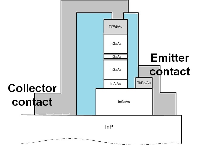
Resonant tunnelling diode (RTD) device cross-section
Resonant tunnelling diodes (RTDs) were first demonstrated in 1974. An RTD consists of vertical stacking of nanometric epitaxial layers of semiconductor alloys forming a double barrier quantum well (DBQW). Typically this consists of two barriers layers of a wide bandgap III-V semiconductor for example AlAs with a thickness less than 2nm with a lower bandgap material sandwiched in between for example InGaAs with a thickness less than 10nm, forming a DBQW structure. However, only with the emergence of precise semiconductor growth technology in the 1980’s, RTDs became more attractive due to the higher performance achieved.
The electrical carrier transport across the DBQW is mainly through resonant tunneling quantum effect. They exhibit two distinct features when compared to other semiconductor devices: negative differential conductance and extremely high frequency (HF) operation. The former corresponds to electric gain: since the DBQW acts as like a Fabry-Pérot interferometer for the charge carriers wave-functions, this gives rise to a N-shaped current versus voltage (I-V) characteristic – the corresponding negative differential resistance (NDR) portion of the I-V characteristic that gives rise to electric gain. The latter, on the other hand, arises from the very thin (a few nanometres) resonant tunnelling structure along the direction of carriers transport, which makes them the fastest pure solid-state electronic device operating at room temperature with working frequencies exceeding 1 THz.
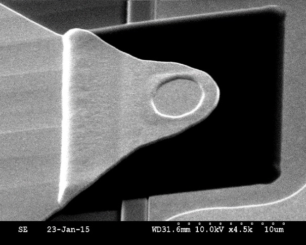
SEM picture of a fabricated RTD with polyimide passivation
These unique features make it possible for RTDs to operate as amplifiers and oscillators, significantly reducing the number of elements required for a given function. Another important characteristic of RTDs is that they can be seamlessly integrated on the same chip with conventional electronic and photonic devices, e.g. transistors, optical waveguides, photodetectors and laser diodes, with potential not only to provide low cost single chip solutions, but also reduced power consumption and increased functionality, speed and circuit reliability, without losing any advantage of using optical devices. Indeed, both electrical-to-optical and optical-to-electrical conversion of microwave signals to/from optical subcarriers, taking advantage of the negative differential resistance and phase-locking properties of RTD devices and oscillators, respectively, has been demonstrated. For these reasons, the RTD will be the underpinning active device technology for iBROW.
III-V ON Si
iBROW RTDs will be based on the Indium Phosphide (InP) material system. This and the other III-V compound semiconductor material, Gallium Arsenide (GaAs), constitute substrates of reference for optoelectronic devices as well as for high frequency electronic circuits This is due to their high electron mobility, peak velocity, larger energy bandgap, breakdown voltage and photonic properties (in particular light generation by laser effect) that cannot be matched by advanced Si or SiGe technology (RF-CMOS and SiGe-BiCMOS, respectively).
Compared to Si, the InP material is expensive and is limited to smaller wafer sizes which makes its processed dies even more expensive. A key project objective will therefore be the integration of the III-V material with silicon (III-on-Si) substrates to reduce the manufacturing costs through the larger wafer diameter sizes and the vastly available silicon manufacturing infrastructure. In addition, this integration will enable the combination of the merits of both III-V and silicon in new functions that would not be possible with any of the technologies alone. On iBROW, both the direct growth and wafer bonding approaches of III-V on Si will be investigated and developed for high frequency RTD electronics and optoelectronics.
COMMUNICATION METHODS
iBROW aims to develop a small scale test-bed for the demonstration of at least 10 Gbps wireless communications between several stand-alone prototype nodes at frequencies around 300 GHz in a near to operational environment. As such, the project aims to identify and evaluate communication technologies and architectures for enabling RTD-based ultra-broadband communications. This aspect of the project will cover modulation formats, communication architectures, and techniques for increasing transmission speed such as massive MIMO.